optical_io
by Andy Sun (achoenix@gmail.com)
Last update: 2026-05-08
Site Navigation
- Homepage
- Silicon Photonics
- Co-Packaged Optics
- Optical Interposer
- Optical Transceiver
- Optical Circuit Switch
- AI Chip
- System Design
License & Citation
NVIDIA CPO
The follow analysis is based on GTC 2025 keynote presented by Jensen Huang.
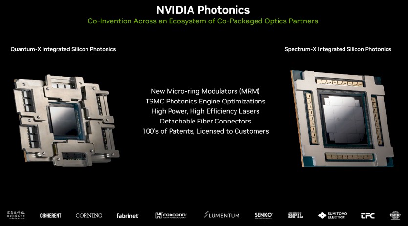
Quantum-X InfiniBand Switch ASIC with CPO
Plan to ship in 2025H2
Features
- 6 CPO socket per GPU (B200/B300?), closer to a NPO concept
- 3 optical engines in each socket
- SerDes running at 224Gb/s per lane with 24Gb as error correction overhead thus 200Gb/s net data rate
- SerDes per ASIC have 72 lanes
- liquid cooling for both the switch core and all optical modules
- 28.8Tbps full duplex bandwidth per switch
- 6 optical subassembly integrated on the switch package’s interposer
- 4.8Tbps of transmit and 4.8Tbps of receive per optical subassembly
- 3 optical engines per optical subassembly
Q3450 System
- 4 Quantum-X chips—provides 115.2Tbps full-duplex bandwidth over 144 ports with 800Gbps
An in-depth analysis is here: NVIDIA Quantum-X CPO
Spectrum-X Ethernet Switch ASIC with CPO (GTC 2025 Keynote)
Plan to ship in 2026H2
Features
- multi-chip module package
- the Ethernet switch ASIC has a monolithic packet processing engine
- 8 SerDes chiplets (two per side)
- 4 unknown chiplets at the corners
- 8 active optical engines (extra 1 spare) on each side, i.g. a total of 32 OEs (36 with spares)
- each optical engine may support at least 1.6Tb/s (equal to the optical engine in Quantum-X)
- same 200Gb/s SerDes, 144 lanes pre ASIC
- liquid cooled
Interconnect Design
Power savings compared to pluggable transeivers
- Pluggable: 30W \@ 1.6Tb/s, i.e. 18.75 pJ/bit
- CPO: 9W \@ 1.6Tb/s, i.e. 5.625 pJ/bit (the optical engine exclude CW laser is 4.375 pJ/bit *)
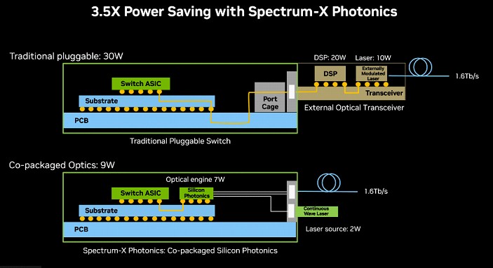
* CW laser power consumption estimation: assuming 12mW is fed to each modulator channel, i.e. 80mW for 8 channels. At least two optical coupling in the link which introduces ~5dB loss, i.e. ~300mW laser output power is required. Assuming the wall-plug efficiency of the laser is ~15% (uncooled at 55C), the laser power is ~2W. Assuming the laser is uncooled and the laser driver has a ~60% conversion efficiency, the overall power of is ~3W, i.e.g ~2 pJ/bit for 1.6Tb/s.
Optical Engine
Ref: NVidia Blog
OE for Quantum-X
- 1.6Tbps PAM4 per OE
- 8 Tx and 8 Rx 200Gbps PAM4 channels, 2 laser output fibers per optical engine
- 200Gbps PAM4 microring modulator per wavelength
- multi-row scaling of optical interconnect throughput within a single package
- Stacked CMOS and photonics components
- Wafer-level integration of micro-lenses
OE for Spectrum-X
- 3.2Tbps PAM4 per OE
- 16 Tx and 16 Rx 200Gbps PAM4 channels, 4 laser output fibers per OE (2x OE per ELS)
- 200Gbps PAM4 microring modulator per wavelength
- solder reflown directly onto the module substrate
- Stacked CMOS and photonics components
- Wafer-level integration of micro-lenses
- detachable optical connector
Challegnes Solved by TSMC
- precise control of the fabrication process
- mitigation of thermal sensitivity
- consistent high-speed modulation
External Laser
Ref: NVidia Blog
Features
- 8 lasers per ELS module
- Quantum-X switch
- 1ELS -> 8 lasers -> 32 lanes: 1 laser per 4-lane
- 4.5 ELS modules per ASIC
- 18 ELS per System (4 ASIC)
- Spectrum-X Switch
- 16 ELS modules per ASIC
- 64 ELS modules per system (4 ASIC)
Challenges Solved
- own dedicated, thermally controlled environment addresses repeated thermal cycling rapidly degrades laser lifetime
- reducing the total number of lasers in the data center by a factor of four compared to legacy designs
- implies 1 laser per 4 modulators (compared with EML), however, the same as the design for Si photonics based modules